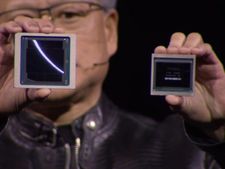
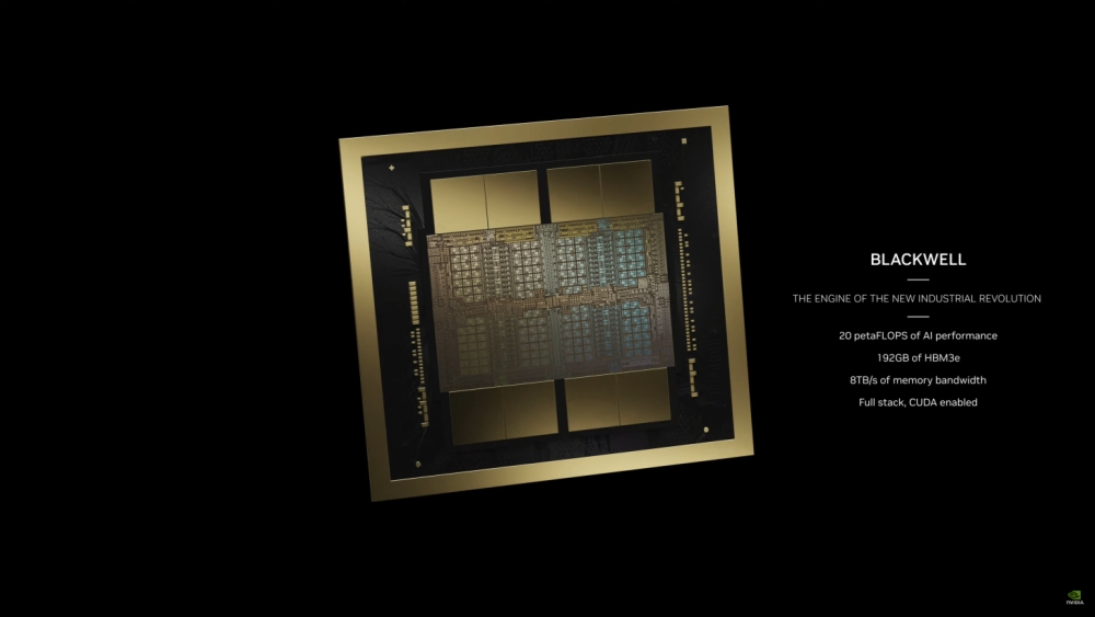
Announced as the "world's most powerful chip" and the largest chip physically possible, the Blackwell is an MCM design with two GPUs connected via a 10TB/s Nvidia high bandwidth interface, making a single unified GPU. It is built on a custom 4NP TSMC process and packs a total of 208 billion transistors, with 192GB of HMB3e memory and 8TB/s of memory bandwidth, as well as full GPU cache coherency. Nvidia says it packs 20 petaFLOPS of AI performance which is a five times higher AI performance compared to the Hopper H100.
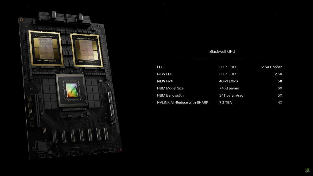
Nvidia went on to compare the new Blackwell GPU architecture fully to the Hopper one, saying it offers 128 Billion more transistors, 5x the AI performance, and 4x the on-die memory. This adds up to to 20 PFLOPS FP8 (2.5x Hopper), 20 PFLOPS FP6 (2.5x Hopper), 40 PFLOPS FP4 (5x Hopper). The HBM model size and bandwidth are at 740 billion Parameters (6x Hopper) and 34T Parameters/sec (5x Hopper), while NVLINK is at 7.2 TB/s (4x Hopper).
In addition, the Blackwell GPU architecture will feature the second-generation Transformer Engine, with micro-tensor scaling support and NVIDIA’s advanced dynamic range management algorithms integrated into TensorRT-LLM and NeMo Megatron frameworks, allowing Blackwell to support double the compute and model sizes with new 4-bit floating point AI inference capabilities. It also uses fifth-generation NVLink, with 1.8TB/s bidirectional throughput per GPU; the new RAS engine, a dedicated engine for reliability, availability, and serviceability; the Secure AI feature; as well as the new Decompression Engine, which should accelerate database queries to deliver the highest performance in data analytics and data science.
In terms of other specifications, the Nvidia Blackwell B200 GPU packs 160 SMs or 20,480 cores, 8 HBM packages for 192 GB of HBM3e memory, has PCIe 6.0 support, and has a 700W peak TDP.
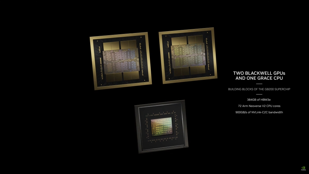
Nvidia will ship the new Blackwell architecture as the Nvidia Blackwell GB200 Grace Blackwell Superchip platform with two B200 Tensor Core GPUs and Grace CPU, connected via a 900GB/s ultra-low-power NVLink chip-to-chip interconnect. It will be available in various systems and server boards, linking up to 72 Blackwell GPUs and 36 Grace CPUs in the NVIDIA GB200 NVL72 rack-scale system, or as the HGX B200 server board with eight B200 GPUs for x86-based generative AI platforms.
All the usual partners are on the list including Cisco, Dell, Hewlett Packard Enterprise, Lenovo, Supermicro, Aivres, ASRock Rack, ASUS, Eviden, Foxconn, GIGABYTE, Inventec, Pegatron, QCT, Wistron, Wiwynn, and ZT Systems.