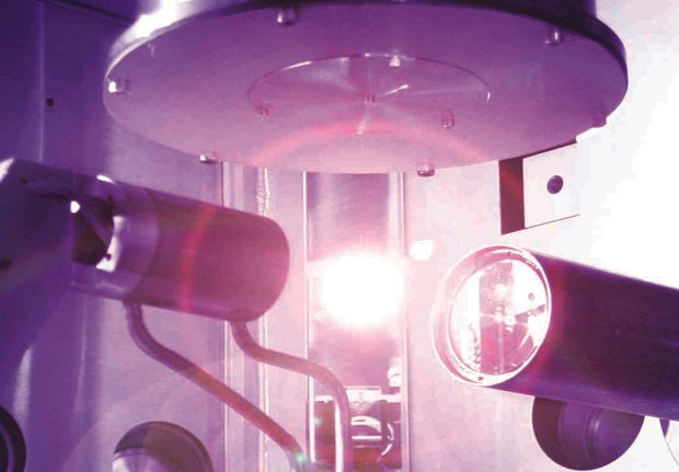
According to Technology Review the technology is ready earlier than expected and the biggest technology hurdles have been overcome. ASML finally has machines out to its customers for test runs, which means that the technology is not far off.
It is still a bit slower than normal lithography, which can pattern 3,000 wafers a day even the normal process is expected to slow down in the coming years because it will need more patterning steps and more expensive masks to make ever finer features on future chips.
EUV technology would have been given up on long ago, if it were not for the fact that no-one else could come up with a better idea. Even now companies are vague above when it will be used in anger.
In 2011, Intel invested $4 billion in ASML, a Dutch chip-making-equipment company and ASML announced that it has overcome the biggest technological hurdle: it hasn’t been practical to switch to the shorter wavelength EUV light because the light sources were far too dim. A dim light source means it takes longer to expose the photoresist this pushes up the cost of making the wafers.
TSMC have hinted it will bring on the technology in 2020. Intel has been less specific, although it claims it is close.


