Index
Page 1 of 10

Review: The best Fermi overclocking potential so far
GTX 465 uses a scaled down version of the GF100 chip; more precisely the chips that haven’t qualified to run on GTX 480 and GTX 470 cards made their way to the GTX 465. Full version of GF100 packs 16 Streaming Multiprocessors (SM) whereas the GTX 465 comes with only 11 SMs and 352 shader processors. Let us clarify – one SM packs 32 shader processors (SPs), or CUDA cores as Nvidia likes to call them. GTX 470 comes with 14 SMs (448 SPs) whereas the GTX 480 comes with 15 SMs (480 SPs). This means that none of these cards use the full potential of the GF100.
The announcement of Fermi GF100 chip also brought about Nvidia’s usage of GDDR5 memory on high-end cards. Unlike AMD, who uses 256-bit memory interface and high-clocked GDDR5, Nvidia uses wider memory bus and slower GDDR5 memory.
Note that the GTX 480 uses 384-bit memory interface (3696MHz memory, 177.4 GB/s bandwidth), the GTX 470 uses 320-bit interface (3348MHz memory, 133.9 GB/s bandwidth) whereas the GTX 465 uses a 256-bit memory interface (3206MHz memory, 102.6 GB/s bandwidth). In comparison, the fastest AMD’s single GPU card, the HD 5870, uses 256-bit memory interface but faster memory (4800MHz memory, 153.6GB/s bandwidth). The HD 5850, which is the GTX 465’s direct competitor, uses 256-bit memory interface (4000MHz memory, 128GB/s bandwidth).
The GF100 is a complex chip made of four Graphics Processing Clusters (GPC), four Raster Engines, six memory controllers, six ROP clusters with 8 ROP units each and, as we said before, 16 SMs. Each ROP cluster is assigned one 64-bit memory controller. The GTX 465 packs 32 ROPs, meaning that compared to the GTX 480, it’s 2 ROPs and two memory controllers short (which at the same time explains the 256-bit memory interface)
Downclocking is the most common and logical way to make a visible difference between cards, but since the GTX 465’s GPU is scaled down in comparison to the GTX 470’s, Nvidia decided to leave the clocks unchanged (607MHz GPU, 1215MHz stream processors). Note that the GTX 480 runs at 700MHz for the GPU and 1401MHz for the shaders.
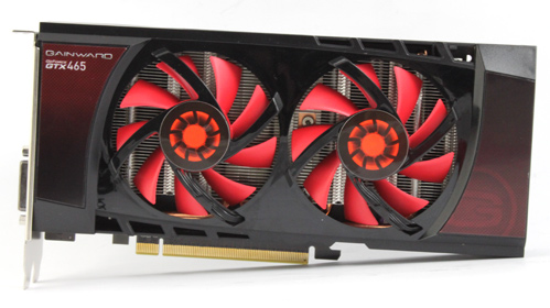
Gainward’s GTX 465 Good card runs at reference clocks and packs a reference video buffer with 1024MB of GDDR5 memory.
GF100 is an extremely fast and powerful graphics processor, but all this comes at a price. Namely, this GPU gets very hot and devising efficient cooling was no easy task. All three Fermi cards use Nvidia’s dual slot cooler which keeps the temperatures in check, but the fans run at a pretty high RPM and it directly translates into noise. Gainward, on the other hand, would have none of that and made its own cooler with two fans. The GTX 480’s TDP stands at 250W; the GTX 470’s is at 215W whereas the GTX 465 comes with a 200W TDP.

Prev Next »
