Index
Page 3 of 9
Today we are finally holding the GTX 480, graphics card based on Fermi architecture. Fermi is the family name for the latest generation of GPUs from Nvidia. The first Fermi derivative is the GF100 GPU - Nvidia’s internal code name for the first Fermi based chip that is used for the GTX 480 and GTX 470 cards. The GF100 is a fairly capable DirectX 11 product manufactured in TSMC's 40nm technology processes with over 3 billion transistors (AMD's RV870, which is used in the ATI Radeon HD 5870, is comprised of roughly 2.15 billion transistors).
Compared to the previous generation GT200, the new GF100 (GTX 480) brings 1.5-3.5x performance gain when compared to the GTX 285 and in addition to greater texture coverage, faster context switching over the GT200, more efficient processing of physics and ray tracing and of course DirectX 11 graphics with unavoidable tessellation which is quite popular these days. According to Nvidia, tessellation is the real reason for the GF100 delay, because Nvidia wanted to have the best implementation.
The biggest advantage of the new GPU is that tessellation and all its supporting stages are done in parallel, enabling high geometry throughput. The GF100 tessellation support is 100% hardware, and isn’t done via software emulation, but even if tessellation is very important for DirectX 11, actual games based on DirectX 11 that utilize the real advantage of all its features are still far away and Nvidia has to prove better performance in current games, and not just in tessellation and upcoming games.
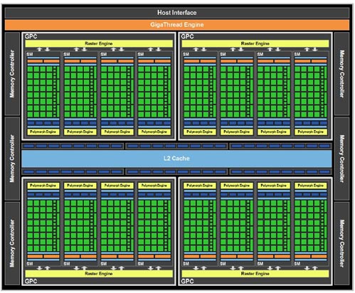
The GF100 GPUs is composed of a scalable array of Graphics Processing Clusters (GPCs), Streaming Multiprocessors (SMs), and memory controllers. The full version of the GF100 chip implements four GPCs, four Raster Engines, 16 SMs with 32 CUDA cores each and six memory controllers, but the GTX 480 comes with 15 SMs with total of 480 CUDA cores and the GTX 470 sports 14 SMs and 448 CUDA cores. Raster Engines operate in parallel compared to a single Raster Engine in prior generation Nvidia’s GPUs.

As you can see and conclude from the picture above, one GPC is a dominant high-level hardware block encapsulates all key graphics processing units representing a balanced set of vertex, geometry, raster, texture, and pixel processing resources, what essentially allows each one GPC to function as a full GPU. GPC includes one Raster Engine (for triangle setup, rasterization, and Z-cull) and up to four SMs (for vertex attribute fetch and tessellation).
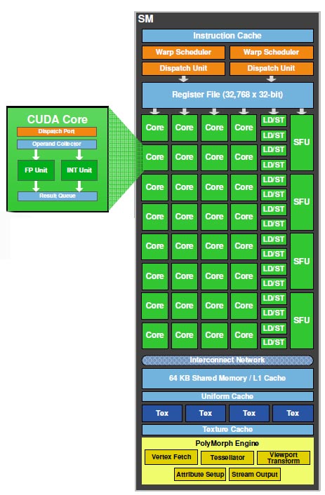
In its full version, the GF100 has 512 CUDA cores, distributed in 16 SM with 32 CUDA processors for each SM. Every Streaming Multiprocessor has its own dedicated PolyMorph Engine, and four dedicated Texture Units (on GT200 GPU, SMs and Texture Units were grouped together in hardware blocks called Texture Processing Clusters (TPCs)).

The PolyMorph Engine performs very different tasks and it has five stages: Vertex Fetch, Tessellation, Viewport Transform, Attribute Setup and Stream Output, thus increasing triangle, tessellation and Stream Out performance. Results calculated in each stage are passed to an SM. The SM executes the game’s shader, returning the results to the next stage in the PolyMorph Engine. After all stages are complete, the results are forwarded to the Raster Engines. By having a dedicated tessellator for each SM, and a Raster Engine for each GPC, the GF100 delivers up to 8x the geometry performance of the GT200. Tesselation factor decides on the number of parts that will a certain object be composed of.

The memory interface is 384-bit wide, but GF100 implements six 64-bit GDDR5 memory controllers (384-bit total) to facilitate high bandwidth access to the framebuffer (the GT200 features a wider 512-bit memory interface, but uses GDDR3 memory).
GF100 has 48 ROP units for pixel blending, antialiasing, and atomic memory operations. The ROP units are organized in six groups of eight. Each group is serviced by a 64-bit memory controller.
On-chip L1 and L2 caches enable high bandwidth transfer of primitive attributes between the SM and the tessellation unit as well as between different SMs. Addition of L1 cache helps to keep as much data on the GPU die as possible, without having to access memory. Each SM has 48/16 KB of shared memory (3x that of the GT200), that can be configured as 48 KB of Shared memory with 16 KB of L1 cache, or as 16 KB of Shared memory with 48 KB of L1 cache (there is no L1 cache on GT200).
