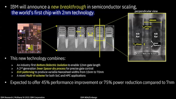
The Tame Apple Press is furious as everyone knows that Apple invents everything these days and has rushed to point out that while the process node is being called '2 nanometers,' nothing about transistor dimensions resembles a traditional expectation of what 2nm might be.
One sniffed only some of the features on this chip are likely to be low single digits in actual nanometers, such as transistor fin leakage protection layers, but it's important to note the disconnect in how to process nodes are currently named.
However, whatever IBM has created seems to be a considerable improvement on what is out there at the moment. IBM said that the performance by is 45 percent at the same power, or 75 percent energy at the same performance, compared to modern 7nm processors.
IBM is keen to point out that it was the first research institution to demonstrate 7nm in 2015 and 5nm in 2017, the latter of which upgraded from FinFETs to nanosheet technologies that allow for greater customisation of the voltage characteristics of individual transistors.
IBM states that the technology can fit '50 billion transistors onto a chip the size of a fingernail' apparently a fingernail is 150 square millimetres. That puts IBM's transistor density at 333 million transistors per square millimetre (MTr/mm^2).
Of course, it is a long way before it gets into the shops. Intel is still struggling to get its 7nm node out the door. And even TSMC doesn’t expect to get to 2nm for some time. It’s currently planning to start early production of its 4nm chip process by the end of the year, with mass production in 2022, per AnandTech. Its 3nm node isn’t expected until the second half of 2022, with 2nm chips still in relatively early development. And all of that assumes that semiconductor companies don’t run into delays — just ask Intel, which has seen any number of manufacturing hiccups over the past decade.


