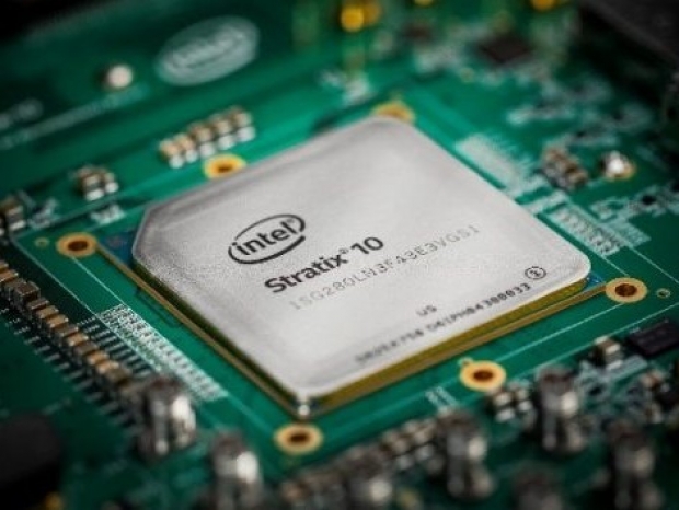
The Stratix 10 is manufactured using an advanced bridging process that logically and electrically stitches together two high-density FPGA dies.
Each die has 5.1 million logic elements, giving the FPGA an extreme density of 10.2 million logic elements to create what Intel claims is the world’s highest capacity FPGA. It has nearly four times the density of its Intel predecessor. Chipzilla said that multiple customers have already received operational samples of the new Intel Stratix 10 GX FPGA,
Intended buyers of the new FPGA include the Application Specific Integrated Circuit (ASIC) prototyping and emulation market, including several companies that build commercial off-the-shelf ASIC systems.
Intel FPGA Vice President of Marketing Patrick Dorsey said prototyping and emulation systems are used by semiconductor companies to verify complex chip designs prior to production to reduce risk.
"Such systems can save semiconductor vendors millions of dollars by helping them identify and eradicate costly hardware and software design bugs before the chips are fabricated”, Dorsey said.
“It’s far more costly to fix hardware design bugs after a chip has been manufactured…Because the risk is so high and the potential savings are so large, these prototyping and emulation systems deliver real, tangible value to IC design teams”, Dorsey said.
Because the new FPGA is so dense, it will require fewer of them in an ASIC, System-on-Chip or an application-specific product set, Intel said. Some integrated circuit designs may include hundreds of millions of ASIC gates.
Intel calls its bonding process EMIB, which is short for Embedded Multi-die Interconnect Bridge technology. The new Stratix FPGA is the first to use the 3D System in Package EMIB to logically and electrically bond two FPGA fabric dies together. Tens of thousands of connections link the two FPGA fabric dies.


