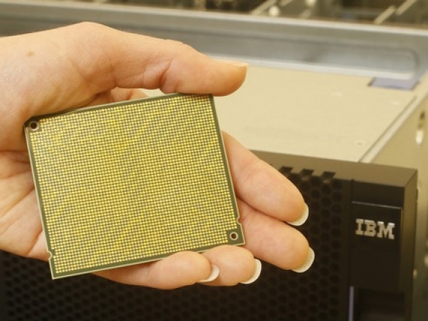
Big Blue boffins are working on an area called 'area-selective deposition' which it thinks might help overcome limitations on lithographic techniques to create patterns on silicon in 7nm processes.
Techniques such as 'multiple patterning' helped ensure integrated circuits kept scaling, but as chips have shrunk from 28nm to 7nm processes, chipmakers have needed to process more layers with ever-smaller features that need more precise placement on patterns.
One of the issues is the alignment between layers which when done badly leads to 'edge placement error' (EPE). In 2015 Intel lithography expert Yan Borodovsky has gone on record saying that it was an issue that lithography couldn't solve.
He suggested that area-selective deposition was a better bet, so IBM's researchers started to check it out.
This might be a successor to EUV lithography, the technique Samsung is now preparing for the fab after decades in the lab.
Rudy Wojtecki, a researcher at IBM's Almaden Research Centre, said that with traditional methods of fabrication, this would require coating a substrate with resist, patterning the resist through an exposure step, developing the image, depositing an inorganic film and then stripping the resist to give you a patterned inorganic material.
"We found a way of depositing this inorganic film much more simply, using a self-aligned process, where we immerse a prepatterned substrate in a solution containing a special material and then add that coated substrate it to a deposition chamber, and you're done. We are literally able to grow a component of a device in a controllable manner at the nanoscale."
The group is using one of three main methods for area-selective deposition called 'atomic layer deposition' with a focus on using 'self-assembled monolayers' (SAMs).
It may help pave the way for hardware that better supports AI applications, such as three-dimensional structures.
"Once we develop methods of scaling this process, we can begin to integrate it as we build next-generation hardware, whether it is for new AI hardware or making devices at the 7nm technology node or beyond", Wojtecki said.
Wojtecki argues his ability to tailor a chemical structure for demanding applications has enabled the development of "new polymerisations, materials and characterisation methods" that may one day become scalable.


