The company spent more than $1 billion to develop the new chip which it claims is as significant as the invention of FPGAs in the 1980s. The outfit believes it can broaden the use of programmable chips across a broad set of applications for the era of big data and artificial intelligence. For deep neural network processing, it could achieve a 20-fold increase in performance.
The ACAP is a dubbed multi-core heterogeneous compute platform which is changed at the hardware level to adapt to the needs of a wide range of applications and workloads. An ACAP can adapt dynamically during operations, and that can make it more efficient in performance and performance-per-watt than central processing units (CPUs) or graphics processing units (GPUs).
Victor Peng, CEO of Xilinx said the ACAP will have 50 billion transistors and will be a significant technology disruption for the industry.
“This revolutionary new architecture is part of a broader strategy that moves the company beyond FPGAs and supporting only hardware developers. The adoption of ACAP products in the data centre, as well as in our broad markets, will accelerate the pervasive use of adaptive computing, making the intelligent, connected, and the adaptable world a reality sooner.”
The ACAP can be used in applications such as video transcoding, database, data compression, search, AI inference, genomics, machine vision, computational storage and network acceleration. Software and hardware developers will be able to design ACAP-based products for the end point, edge and cloud applications.
Talking to Venture Beat, Peng said that it can do very intricate system designs and still have that flexibility in programming.
“You can still change things in the design at the last minute as protocols change.”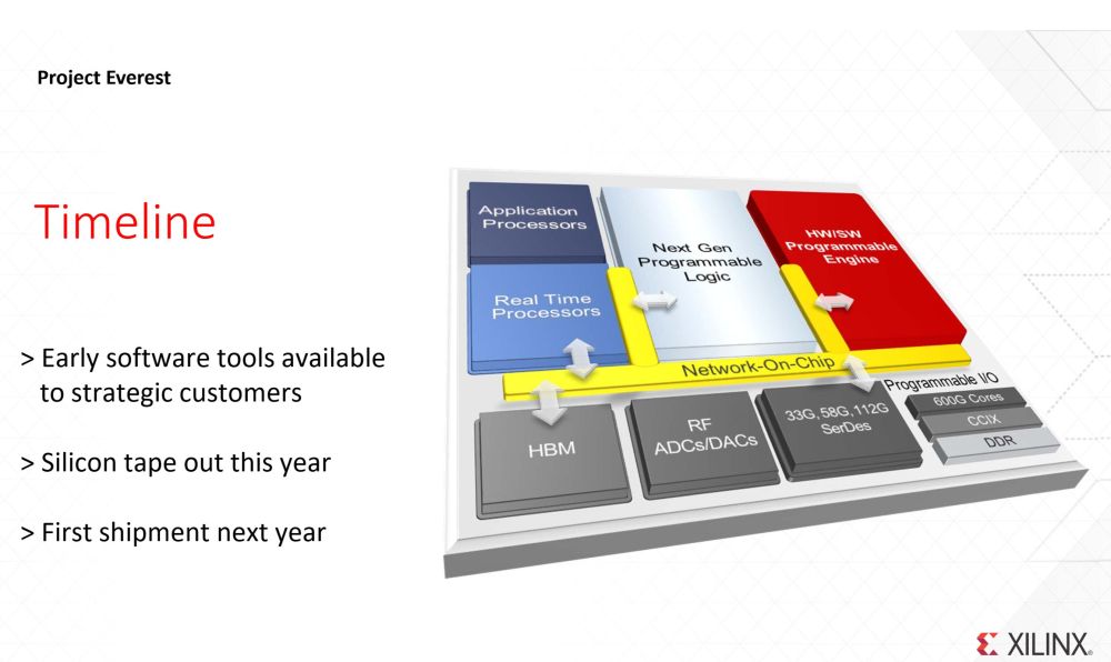
The first ACAP product family, codenamed Everest, will be developed in a 7-nanometer manufacturing process in TSMC factories for production later this year.
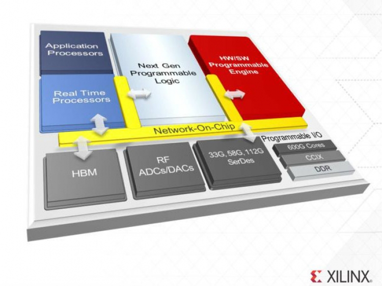
An ACAP has – at its core – a new generation of FPGA fabric with distributed memory and hardware-programmable digital signal processor (DSP) blocks, a multicore system-on-chip, and one or more software programmable, yet hardware adaptable, compute engines, all connected through a network on chip (NoC). That means it has a lot of built-in hardware capability that is programmable.
ACAP has been under development for four years at an accumulated R&D investment of $1 billion. There are currently more than 1,500 hardware and software engineers at Xilinx designing ACAP and Everest. Software tools have been delivered to key customers. Everest’s design will be done in 2018, and the company plans to ship chips in 2019.
Everest is expected to have a 20 times performance improvement on deep neural networks compared to today’s latest 16-nanometer FPGA chip. Everest-based 5G remote radio heads will have four times the bandwidth versus the latest 16-nm-based radios.