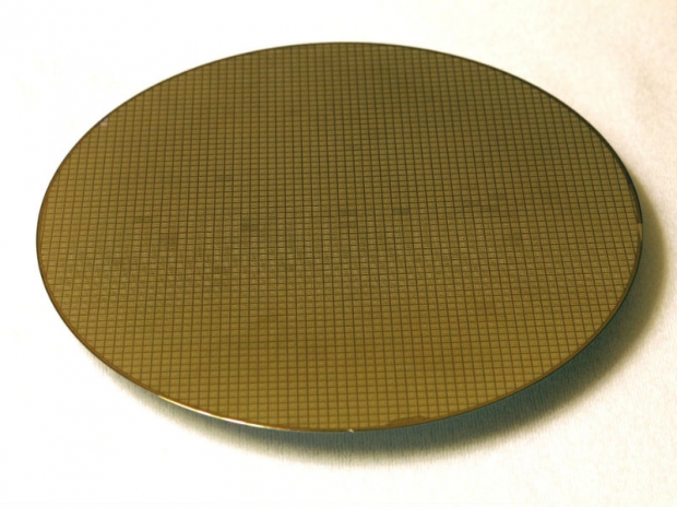
This is the second generation 10nm manufacturing process, and of course it will be more mature then the first one. It also features enhancements to the 3D FinFET structure reducing the leakage between the transistors. Samsung also confirmed that it was the first company to begin mass production of system-on-chips (SoCs) products on 10LPE last October. Yes, that was the Snapdragon 835.
Samsung expects a 10 percent performance gain and a 15 percent power consumption reduction which will definitely help the next generation SoCs. One can expect that the successors of Snapdragon 835 that some call Snapdragon 845 and the next generation Exynos - let’s call it the 8900 series that targets the Galaxy S9 phone - will be manufactured using this process.
Samsung is currently installing the manufacturing equipment for the 2nd generation 10nm Low Power Plus in Hwaseong, Korea and it is expected that the first chips will leave this fab before the end of Q4 2017. This is just in time for the Galaxy S9 and other Android spring refresh phones that usually get announced in Q1 and ship in early Q2 of the year.
As you can imagine this is too late for the next generation iPhone that many call the iPhone 8, as this needs to have millions of SoCs manufactured by mid-summer this year. Therefore many expect that TSMC might be the only supplier for the A11 iPhone SoC.
Ryan Lee, Vice President of Foundry Marketing at Samsung Electronics said:
“With our successful 10LPE production experience, we have commenced production of the 10LPP to maintain our leadership in the advanced-node foundry market. 10LPP will be one of our key process offerings for high performance mobile, computing and network applications, and Samsung will continue to offer the most advanced logic process technology.”


