The new test chip contains ARM's yet-to-be-announced "Artemis" CPU core which is named after a goddess who will turn you into deer and tear you apart with wild dogs if you ever see her. [The NDA must have been pretty tough on this chip.ed]
In fact things have been ticking along on this project for ages. ARM discloses that tapeout actually took place back in December last year and is expecting silicon to come back from the foundry in the following weeks.
ARM actually implemented a full four-core Artemis cluster on the test chip which should show vendors what is possible for their production designs. The test chip has a current generation Mali GPU implementation with 1 shader core to show vendors what they will get when they use ARM's POP IP in conjunction with its GPU IP. There is also a range of other IP blocks and I/O interfaces that are used to validation of the new manufacturing process.
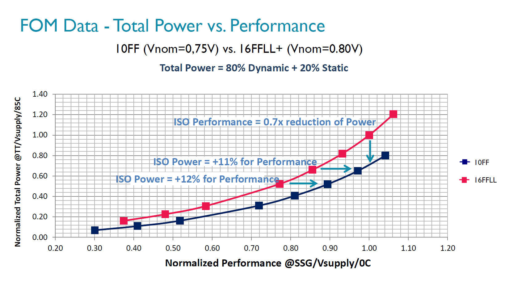
TSMC's 10FF manufacturing process is supposed to increase density with scalings of up to 2.1x compared to the previous 16nm manufacturing node. It also brings about 11-12 per cent higher performance at each process' respective nominal voltage, or a 30 per cent reduction in power.
ARM siad that comparing a current Cortex A72 design on 16FF+ and an Artemis core on 10FF on the new CPU and process can halve the dynamic power consumption. Currently clock frequencies on the new design are still behind the older more mature process and IP, but ARM expects this to improve as it optimises its POP and the process stabilises.


