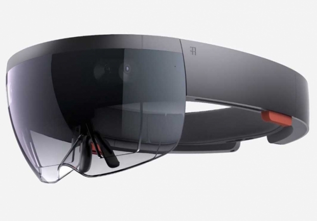
Although hacks have been allowed to play with Vole’s Hololens details of its special Holographic Processing Unit (HPU) have been as mysterious as Donald Trump’s hair.
At the Hot Chips conference in California Microsoft devices engineer Nick Baker provided a presentation on exactly what's inside the HPU and how powerful it is.
This turns out to be a TSMC-fabricated 28nm coprocessor that has 24 Tensilica DSP cores. It has around 65 million logic gates, 8MB of SRAM, and an additional layer of 1GB of low-power DDR3 RAM.
The RAM is separate from the Atom Cherry Trail which has its own 1GB. All up this means that the HPU itself can handle around a trillion calculations per second.
The power is low too – less than 10W from the power supply to handle gesture and environment sensing, PCIe and standard serial interfaces.
Vole has 10 custom instructions to speed up special instructions made by HoloLens for its augmented reality algorithms.
The Verge has done a tear down of it all here


