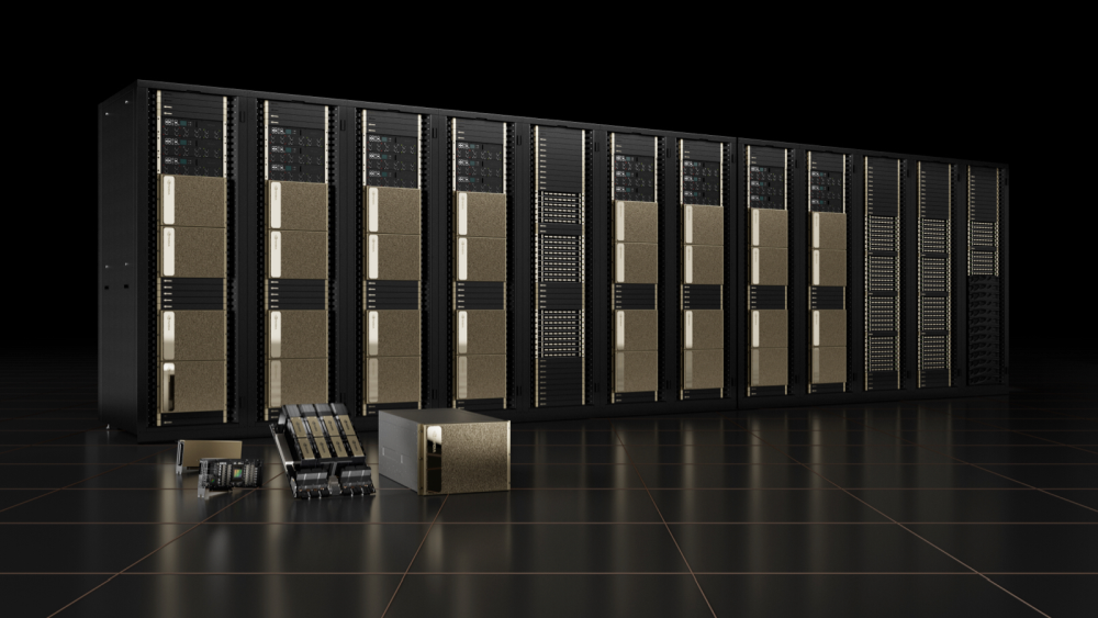
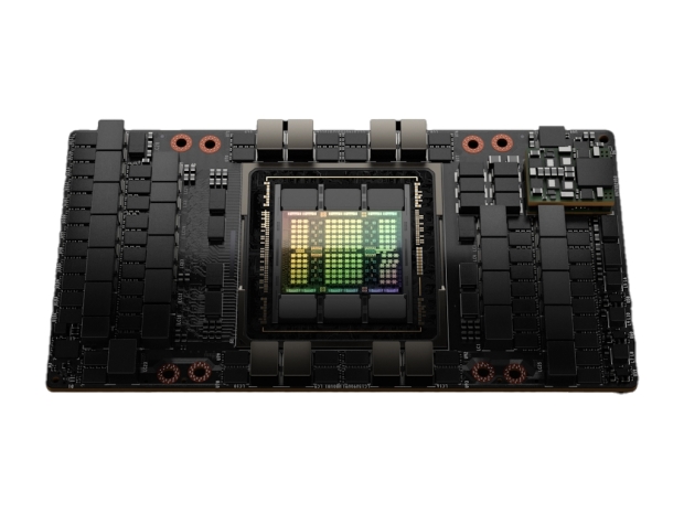
Nvidia had its eye on datacenters for quite some time and according to Nvidia founder and CEO Jensen Huang, these "re becoming AI factories -- processing and refining mountains of data to produce intelligence. Nvidia H100 is the engine of the world's AI infrastructure that enterprises use to accelerate their AI-driven businesses."
Nvidia has released a rather extensive whitepaper detailing its Hopper architecture, the GH100 GPU, and the H100 accelerator, and there is a lot of things to consider before comparing it to the previous generation Ampere-based A100 accelerator.
Some things that Nvidia was keen to note about the GH100 monster is the fact that it is built on what Nvidia calls a custom version of TSMC's 4nm manufacturing process, packs 80 billion transistors, and has impressive performance improvements.
Some of the key architecture improvements include new Hopper Tensor cores with Transformer Engines, a specialized type of tensor cores designed to accelerate ML models, new DPX instructions with dynamic programming for GPUs, NVLink 4 with 900GB/s bandwidth per chip, and more.
The fully-enabled GH100 GPU (since the H100 accelerator uses a somewhat cut-down version), packs 144 SMs, or a total of 18,432 CUDA cores, and although Nvidia did not disclose size details, it is possible that Nvidia managed to pack those 80 billion transistors on a similar size to GA100, of just above 800mm2. The GPU has 128 FP32 CUDA cores per SM, and can pack up to 80GB of HBM3 memory with 3TB/s of memory bandwidth.
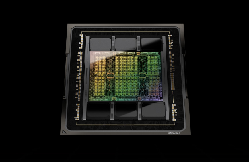
The H100 accelerator gets new SXM5 interface, packs 16896 CUDA cores and has up to 80GB of HMB3 memory
As was the case with previous Nvidia accelerators, the H100 accelerator is based on a somewhat cut-down version of the GH100 GPU with 132 SMs, or a total of 16,896 CUDA cores, at least in the SXM5 board form-factor for the high-performance servers. The PCIe card version for mainstream servers will end up with 114 SMs, or 14,592 CUDA cores.
According to Nvidia's own specifications, we are looking at 528 Tensor cores for the H100 with 80GB of 4.8Gbps HBM3 memory on a 5120-bit memory interface, peaking at 3TB/s of memory bandwidth. It is capable of pushing 60 TFLOPS of FP32 and 30 TFLOPS of FP64 vector compute performance.
The SXM5 version has a TDP of 700W, while the PCIe version peaks at 350W.
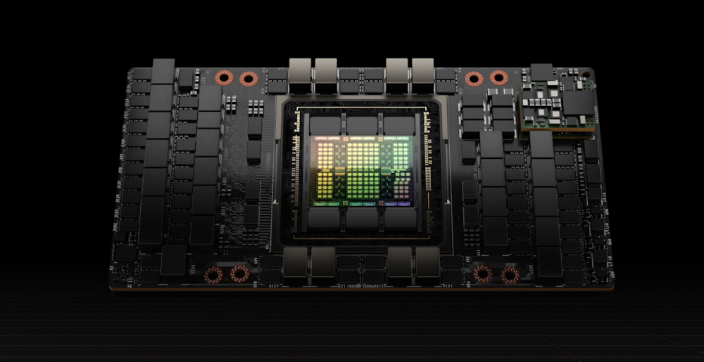
Nvidia has updated its HGX baseboards with H100 and we are probably looking at the same 4-way, 8-way, and 16-way multi-GPU designs as with the A100 GPUs.
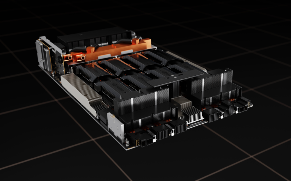
According to Nvidia, H100-equipped systems will be available in Q3 2022, including DGX and DGX SuperPod servers, as well as HGX servers from OEM partners.
