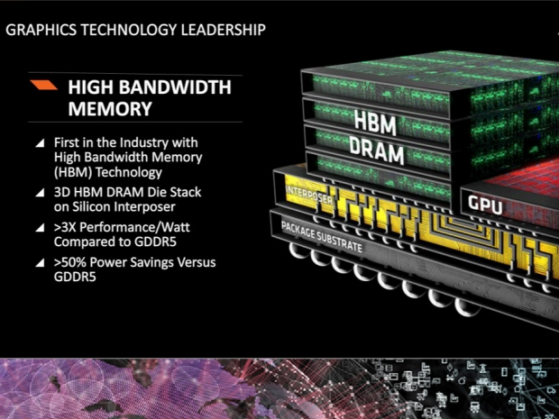
We have already mentioned that Greenland-based graphics will get second generation HBM 2.0 that has double the bandwidth and that can easier get two times the memory. HBM 2.0 has a much larger frame buffer at double the bandwith of the HBM 1.0. The HBM 1.0 will see the light of the day with Fiji GPU-based graphics cards (Radeon R390 is the name that we saw around but can not confirm.)
The first generation of HBM, also called HBM1, supports 2Gb per DRAM die, 1Gbps speed per pin, 128 GB/s bandwidth and 4 Hi Stack of 1GB.
The second generation High Bandwidth Memory (HBM) will multiply these numbers to 8Gb per DRAM die, 2Gbps speed per pin, 256 GB/s bandwidth and Four Hi Stack of 4GB or 8 Hi Stacks of 8GB per chip. The second generation HBM is more attractive and it makes sense for Nvidia to wait for it for its Pascal chips.
AMD with a Fiji GPU will have 4GB memory with four chips and 8GB with dual chip configuration while the Greenland GPU will have a theoretical limitation increased to 32GB for single and 64GB HBM second generation memory for the dual GPU card.
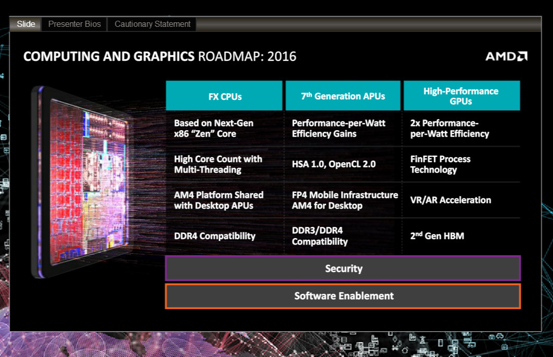
What Mark Papermaster confirmed was that the next generation 2016 GPU core supports second Generation HBM as well as FinFET process technology. In AMD's world, FinFET can mean TSMC 16 nm manufacturing or GlobalFoundries 14nm but Papermaster didn’t follow up with any clarification to the 2016 slide.
Since there is a Fiji VR a dual GPU version of the HBM powered graphics card coming, AMD will continue to push for Virtual Reality (VR). This might be a way for AMD to return to the high end – high margin and profitable part of the market. AMD's Liquid VR supports Oculus VR, HTC – Valve Re Vive VR glasses. Since the slide indicates that 2016 AMD graphics supports Augmented Reality we believe that Fiji and Greenland 2016 graphics support Microsoft Hololens as well.
Papermaster claimed 2016 GPUs will have two times increase in performance per watt efficiency. Transistors in 14 / 16nm GPUs can end up some 4 times smaller and we would expect huge increase in performance per watt with the new architecture.
AMD didn’t go into more details, but it is likely that the future graphics card will be based on 14/16 nm FinFET manufacturing process with second generation HBM memory, two times higher performance per watt and VR / AR acceleration as a main goal. It will run games at incredible FPS too.


