It is still unclear whether or not Fiji can end up faster than the Titan X card, but our sources are certain that there is a way to make Fiji XT compatible with HBM2 (second generation High Bandwidth Memory).
HBM2 won't work out of the box with Fiji, but since this memory will become widely available at a later date, probably toward the end of the year, AMD has enough time to get ready. The only question is wther the Fiji XT architecture will stay competitive enough to fight Nvidia's Pascal GPU that we expect toward the end of the year, or in early 2016. If AMD needs more peformance to take on Pascal until it has a new GPU of its own, Fiji XT implemented as two GPUs in a Crossfire mode on a single PCB should do the trick. If this turns to be the case, it will win in some benchmarks, but due driver limitations it won't win them all. AMD's Virtual Reality focus is something to consider, and with that in mind a dual-GPU on a single PCB makes sense.
HBM2 doubles the bandwidth
It is not clear if Fiji needs another revision to support HBM2, or if a simple PCB revision will do the trick, but the company will make necessary adjustments in order to support the second generation of this super-fast memory for the Fiji XT core.
4-HI HBM1 has a 1024-bit interface, can handle two prefetch operations per IO and has a maximum bandwidth of 128GB per second. The tRC is 48nm, with tCCD of 2ns (1tCK), and the VDD voltage of 1.2V. For example GDDR5 has 1.35 to 1.5V and a top bandwidth of 28GB/s throughput per chip.
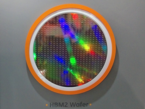
The 4-Hi HBM2 solution, according official SK Hynix data provided to Fudzilla, has 1024 bit I/O, two prefects operations per IO, and 64 Byte access granularity (=I/O x prefetch). The maximum possible bandwidth with HBM 2 doubles to 256GB per chip at the same 48nm tRC, with tCCD of 2ns (1tCK), and the VDD voltage of 1.2V.
With four HBM1 chips on an interposer in 4-Hi HBM1 (16 Gb) you can expect up to 8GB per card, while this figure doubles with HBM2 to 32 Gb per memory die, or 16GB total with four chips.
We are not sure if the next generation Greenland GPU uses HBM1 or HBM2.


