The card is expected in the second part of 2015, and it will beat Nvidia Pascal to market. Nvidia is also using High Bandwidth Memory (HBM) for its 2016, 16nm GPU, but the company is using another technique, quite different compared to AMD's Fiji. Nvidia also announced Pascal Unified memory with 3D memory, an NVLink GPU in 2016 pointing to a Stacked DRAM powered Volta, the successor of Maxwell. Pascal is next year, as Nvidia needs to have a 16nm TSMC node operational and ready before it goes after this next big thing.
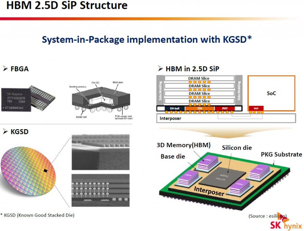
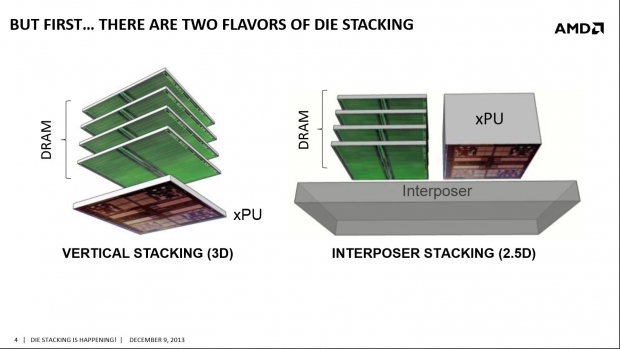
AMD is using what is calls a 2.5D-IC silicon interposer, which means that there will be two separate chips on the same silicon interposer and package substrate. Fiji in 28nm will be one of these chips, and the second batch of chips will be the High Bandwidth Memory (HBM) memory designs. However, there is a catch with AMD's approach.
From what we've learned, Fiji is limited to 4GB memory. With the current memory technology the GPU would simply be too big to put on an interposer and package. The interposer should be viewed as a stack of conductors that lets the GPU and HBM memory communicate at much higher speeds than ever before. The interposer then gets into the package that goes on PCB. You could say the interposer is the middle-man that makes things faster.
Hynix has HBM memory with 1024-bit wide interface and 1Gb/s per pin data-rate. This results with 128GB/s bandwidth per memory chip. In case of four 8 Gb chips (1GB) with a 1000MHz core clock you can end up with total bandwidth of 512GB/s. There are indications that HBM memory on Fiji might work at 1.25GHz, which would result in 640 GB/s. The Geforce GTX 980 has 224GB/s bandwidth, while Geforce Titan Back has 336 GB/s.
SK Hynix has listed that 1GB, 128GB/s chips with 1.0Gbps speed packaged in 5mKGSD are available now, January of 2015. These HBM chips feature 4Hi stack VDD/VDDQ 1.2V. The old GDDR5 needs 1.5V to work, meaning that HBM is not only faster, it is more power efficient as well. Fiji could end up having more than twice the bandwidth or Nvidia's current and upcoming Titan cards.
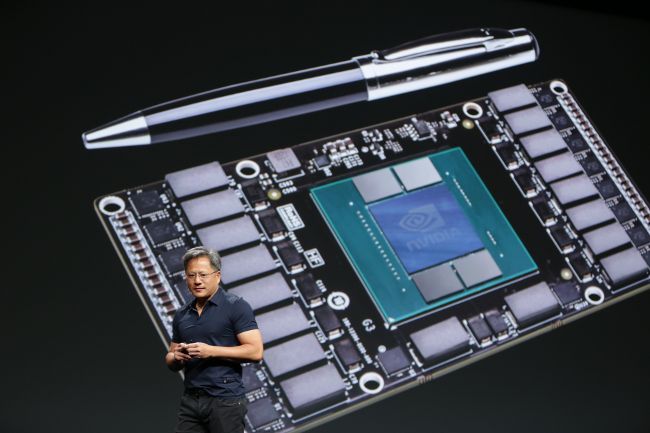
Nvidia on the other hand is using what is called Vertical stacking 3D, or on-package stacked DRAM for its Pascal 2016 GPUs. Nvidia gives a straightforward explanation of the meaning of 3D memory on Pascal: "3D memory: Stacks DRAM chips into dense modules with wide interfaces, and brings them inside the same package as the GPU."
The clear benefits are a massive increase in bandwidth and quadruple energy efficiency. Nvidia is waiting for 16nm to make such a chip possible, and 3D memory is better approach than the interposer.
Back to the AMD Fiji approach with 2.5 stacking and interposer. Our sources claim that you cannot put more than four memory chips on the interposer, meaning that Fiji is limited to 4GB of memory. Eight chips next to a massive GPU would result in massively big chip (remember the GPU and memory chips are on the same board - interposer) and then put on the package. This is why we don’t think 8GB HBM Fiji will happen with this generation, but with time Hynix will come with more dense HBM memory chips making 8GB 2.5 D cards possible.

The only thing that comes to mind is that AMD could be using 4GB HBM memory on the interposer and then put some additional GDDR5 chips on the PCB. Think of it as L2 and L3 cache with some older CPUs. Level two cache would be really faster, while Level tree cache would be slower, but would be able to get some important things done.
We don’t think that this would happen as GDDR5 memory would be significantly slower than the HBM part, making the similar case than with Geforce GTX 970 memory. Fiji has a good chance to beat whatever Nvidia comes up with in 2015, but it will probably have a hard time fighting against Pascal. Pascal is coming in 2016 and one can only hope that it will happen in early 2016.
We believe Fiji and Pascal will enable single GPU 4K gaming at acceptable frame rates and prices.


