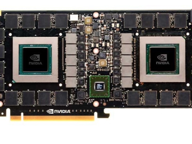
In fact based on what Nvidia says the H100 NVL (H100 NVLink)will be a rubbish card for gaming and targets the growing AI market.
From the information and images Nvidia has released, the H100 NVL will have three NVLink connectors on the top, with the two adjacent cards slotting into separate PCIe slots. This will accommodate servers that don't support Nvidia's SXM option, with a focus on inference performance rather than training.
The NVLink connections should help provide the missing bandwidth that NVSwitch gives on the SXM solutions, and there are some other notable differences as well.
Previous H100 solutions such as the SXM and PCIe came with 80GB of HBM3 memory, but the package contained six stacks, each with 16GB of memory. What we do know is that the H100 NVL will come with 94GB per GPU, and 188GB HBM3 total.
Total performance is double that of the H100 SXM: 134 teraflops of FP64, 1,979 teraflops of TF32, and 7,916 teraflops FP8.
It has the same core design of the H100 PCIe, which also supports NVLink, but potentially now with more of the GPU cores enabled, and with 17.5 per cent more memory.
It looks a bit pricey too. Some punters suggest that it could cost $80,000 for a pair of H100 NVL.


