Any processor, SoC or GPU you think of, Nvidia, AMD, Intel or Qualcomm, Apple, Samsung are predominantly using Xilinx chips to prototype their hardware silicon designs before they get them to the fabs for production. Design of an ASIC usually takes a few years, and FPGA enables software engineers to start writing and testing the code before the hardware ASIC has been taped out and produced. Hardware engineers can also test and analyze their designs before they go to production and potentially fix the errors before they get to silicon design.
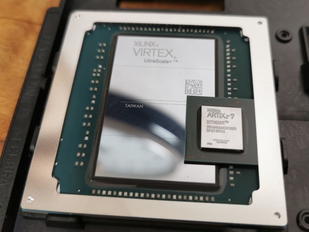
The new Virtex Ultrascale+ VU19P features nine million system logic cells catered for larger and more complex designs. To be a bit more precise, Xilinx has customers among most ASIC and SoC manufacturers who use FPGAs for emulation, prototyping and validation of their designs in 5G, automotive, and AI as well as next-generation test equipment.
The U19+ FPGA chip also supports 80 high-speed transceivers for high port density test equipment, an important step in the design of any chip. VU19P comes with 2,072 user I/Os for multi-FPGA interconnect, and this is important as any of the emulations requires more than one FPGA.
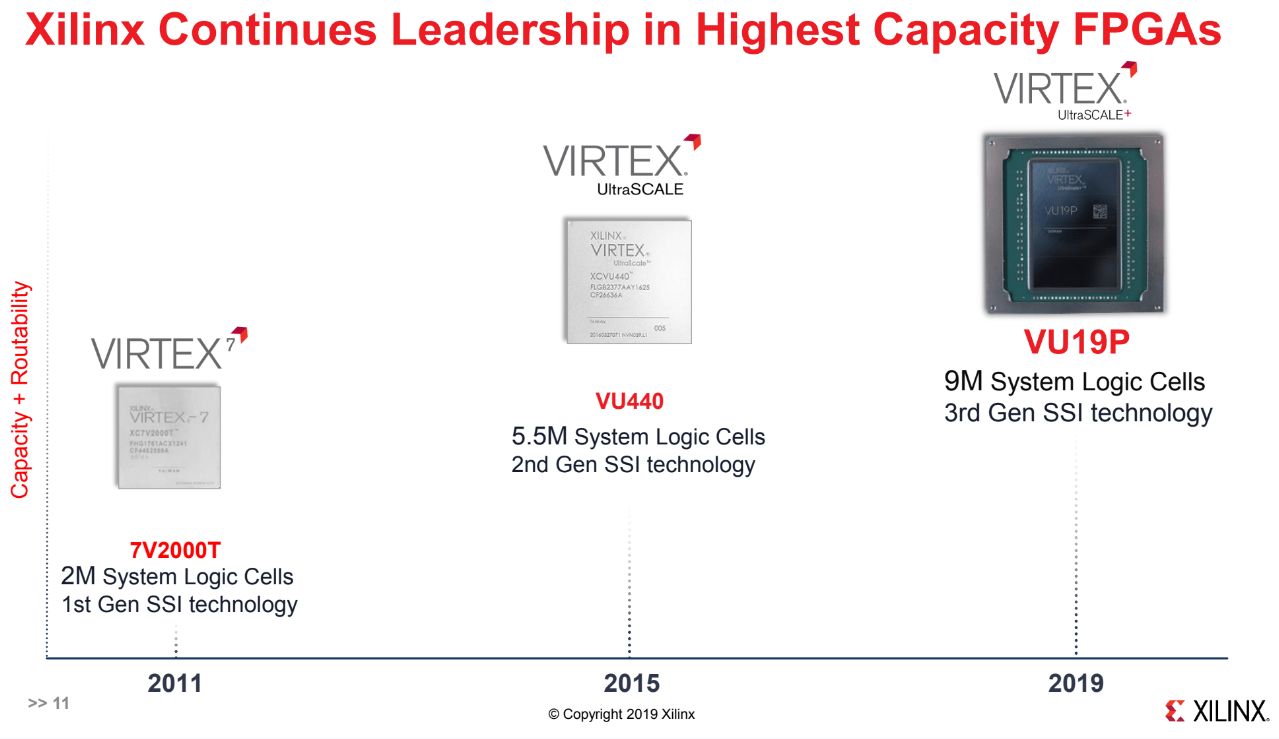
The Virtex Ultrascale+ FPGA VU19P can emulate 16 Cortex A9 chips and the previous generation Virtex UltraScale VU440 FPGA was able to emulate just 10. The system logic count was increased by 1.6 times from 5.5 million in VU440 to 9 million with VU19P.
The total I/O bandwidth grew by 1.4 times featuring 2,072 user I/Os for multi-FPGA interconnect with 1.5 Tb/s I/O bandwidth. Many customers will use multiple VU19P to emulate a more complex ASIC design. The world’s largest FPGA supports 80 high-speed 28G transceivers for high port density test equipment. The total bandwidth of these transceivers sits at 4.5Tb/s. The number of transceivers grew by 1.7X while the transceivers bandwidth increased 2.9 times from the previous generation. 
VU19P comes four years after VU440 or its previous generation, and this is the third generation Stacked Silicon Interconnect technology. Just for reference, the first generation 7V2000T from 2011 used two million logic programmable cells, 4.5 times less than the 2019 VU19P.
Once again, the VU19P will emulate real-world products, and it is a powerful vehicle for emulation and prototyping in 5G, automotive, and AI as well as next-generation test equipment.
As hardware is nothing without software, Xilinx has covered that part too.
The 3rd generation development platform named Vivado is designed from the ground up for emulation-class design support.
It includes Tools and IP with automated design closure assistance, interactive suggestion, and design tuning. Compile-time and Quality of results include multi-generational compile time improvement, as well as robust debug support.
The VU19P will be available in fall, 2020.


