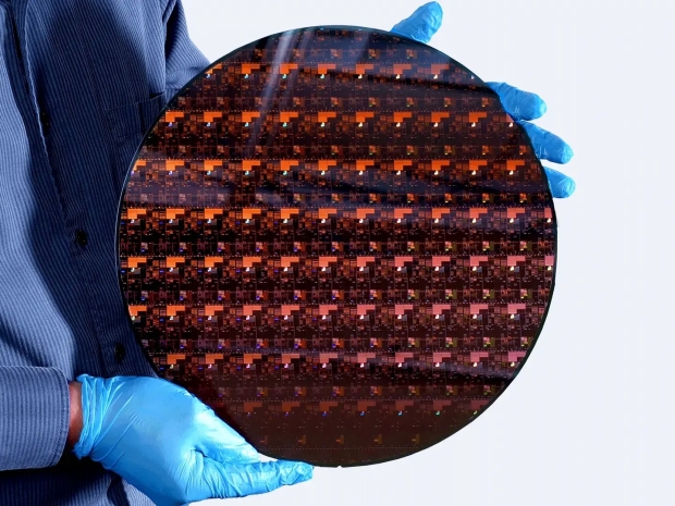
The new production node is expected to deliver between 24 and 35 per cent power reduction, or a 15 per cent performance improvement at the same voltage, along with a 1.15X increase in transistor density compared to the previous 3nm process.
Most of these improvements stem from TSMC’s introduction of gate-all-around (GAA) nanosheet transistors, alongside its N2 NanoFlex design-technology co-optimization (DTCO) and other cutting-edge innovations that were highlighted at IEDM.
TSMC claims GAA nanosheet transistors offer enhanced flexibility, enabling designers to adjust channel widths for a more balanced performance-to-power ratio. This design flexibility is bolstered by N2 NanoFlex, which allows for the creation of short cells with minimal area and
range, achieved via the company’s third-generation dipole-based integration, offers additional fine-tuning, combining both n-type and p-type dipoles for optimal results.
The N2 process also includes a range of refinements at improved power efficiency, or tall cells optimised for maximum performance.
The outfit claims that using six voltage threshold levels (6-Vt) spanning a 200mV the process and device levels. These innovations aim to enhance transistor drive currents by optimising sheet thickness, junctions, dopant activation, and stress engineering.
Effective capacitance (Ceff) is reduced, resulting in industry-leading energy efficiency. Together, these advancements deliver impressive I/CV speed gains of approximately 70 per cent for N-type and 110 per cent for P-type nanosheet transistors, TSMC says.
TSMC claims its N2 node outperforms FinFET technology at low supply voltages of 0.5V to 0.6V, providing a notable increase in performance per watt. These process and device optimisations boost clock speeds by about 20 per cent, while standby power consumption is slashed by approximately 75 per cent when operating at 0.5V.
The integration of multiple threshold voltage options, coupled with N2 NanoFlex, allows for even greater design flexibility, particularly for energy-efficient processors in high logic density applications, the company said.
The advancements in transistor architecture and DTCO are particularly significant for SRAM scalability, a challenge faced by leading-edge nodes in recent years. With N2, TSMC has achieved a record-breaking 2nm SRAM density of around 38Mb/mm².
If TSMC is telling the truth, its power consumption has been reduced. The tighter threshold voltage variation (Vt-sigma) of the GAA nanosheet transistors leads to a 20mV reduction in minimum operational voltage (Vmin) for High Current (HC) macros and a 30–35mV reduction for High Density (HD) macros when compared to FinFET-based designs. These improvements enable stable SRAM read and write functionality down to approximately 0.4V, maintaining strong yields and reliability.
TSMC claims to have integrated new middle-of-line (MoL), back-end-of-line (BEOL), and far-BEOL wiring technologies that reduce resistance by 20 per cent. The MoL now features barrier-free tungsten wiring, which decreases vertical gate contact (VG) resistance by 55 per cent, resulting in a 6.2 per cent increase in ring oscillator frequency. The first metal layer (M1) has also been optimised, created using one extreme ultraviolet (EUV) exposure pass followed by a single etch step (1P1E).
TSMC said this simplification reduces complexity, lowers mask counts, and enhances overall process efficiency, saving several EUV masks. The use of EUV 1P1E for M1 cuts standard cell capacitance by nearly 10 per cent.
TSMC has introduced features for high-performance computing (HPC) applications. The N2 process includes super high-performance MiM (SHP-MiM) capacitors, which provide around 200fF/mm² of capacitance, enabling higher maximum operating frequencies (Fmax) and reducing transient voltage droop, thus optimising performance in demanding HPC environments.


