Page 3 of 3
Layout:
This board is clearly targeting the high end market. With tons of accessories and some unique features it seems possible it will reach the €200 price-target.
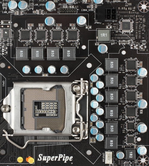
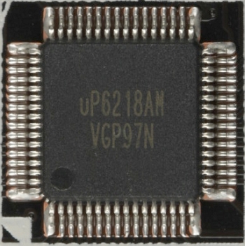

The VRM is an analog 8-phase design and as expected it features highly integrated MOSfets. For some reason MSI is using uPI VRM controllers. It seems this company did impress MSI. We have to wait and see. The northbridge portion is driven by a two-phase design.
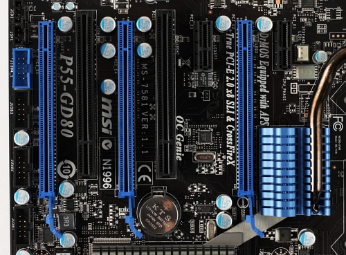

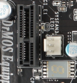
The slot design is very straightforward. Three PCIe 2.0 x16 slots are a bit hefty for our taste, because the most two-slot graphics-cards will block all but one PCI and PCIe slot. Lynnfield only supports one PCIe x 16, so using Crossfire or SLI sets you back to 2x x8. The third PCIe x16 slot comes from the PCH which allows only for x4 speed. One of the problems with the board is the fake northbridge cooler which will block the first PCIe x1 slot. We can't understand what benefit it should bring and what massive heat it should dissipate. We think it's a waste of money, yes your money, because it's 100 percent unnecessary. One special feature is the single segment LED which shows how many phases are in use. A nice gimmick but we think not located on the right spot on the board.
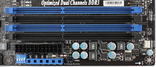
The memory slots are at a safe distance to the CPU socket but the power connector is really close. That is because MSI included a new feature called "V-Check" where you can take measurements of some voltages on the board if you have a multimeter.
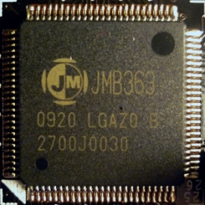
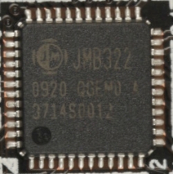
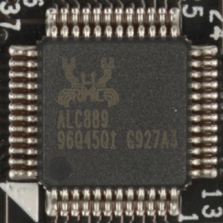
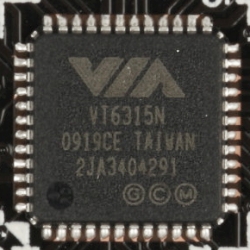
For some reason all vendors go for the cheapest PCIe Gb LAN solution on the market, which is the recently introduced Realtek RTL8111DL. It's an improvement over the RTL8111C and now supports 9k Jumbo Frames, but still Realtek is not known for very good performance, especially the I/O load is quite weak. A Marvell, Broadcom or Intel chip would have been a better choice, but of course opting for a better chip would also have increased costs. Because this is a high end board we had expected something better. Also the JMB363 is quite standard, it supports one PATA, and two SATA ports. One SATA port is used one the backpanel, so a JMB322 does multiply the remaining port. Of course that is not a very good solution if you will use both of them. Next time MSI, please remove such useless ports, and use a JMB362 for two eSATA ports. We think PATA ports are obsolete. The audio portion is provided by a standard Realtek codec, this time an ALC889. It's an improved version of the ALC888, but with higher signal-noise ratio and decoding capabilities for DTS and Dolby. At least MSI went the extra length and used a VIA PCIe Firewire controller.

The PATA and SATA connectors are on the edge of the board and all of them are angled at 90°. This is the best solution available because the connectors won't interfere with any cards.
Conclusion
MSI did the most things right and some things not that well, but of course we would always like to see the perfect board.
Due to the fact we still don't have any LGA1156 CPUs, you'll have to wait for benches.
« Prev Next
