Index

Review: Fast, pricey and hot
We've been waiting, and waiting and waiting some more, but today the wait is over for the most part. This is probably second most controversial if not the most controversial chip in Nvidia’s history and we must admit we haven’t seen such lousy execution with so many delays since the NV30 days.
You might recall that Fermi was supposed to launch in November, then December and then it was finally pushed for the last days of March. Back in November Nvidia did make an A2 silicon that was ok, but could not clock at desired speeds and the company decided to wait for A3 and make things right.
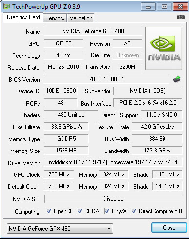
The final GPU clock is 700MHz. Shaders, or GPU CUDA cores as Nvidia calls them, run at 1401MHz and the GDDR5 memory runs at 1848MHz. Its 12 memory chips pack a total of 1536MB of GDDR5 memory. The memory comes from Samsung and and it's designated K4G10325FE-HC04. These can be traced as specified to run at 1250MHz (5000MHz effective). The card also features a CHiL branded voltage regulator which happily supports voltage adjustments.
The memory interface is 384-bit, something that we’ve seen before. The chip has 480 cores and its quite clear that Nvidia had to trim the chip from the original 512 cores to get better yields. Nvidia tells everyone that it expects good availability but this is yet to be seen as the card should be on the shelves by April 12th.
The TDP of 250W is the highest in the GPU history but Nvidia’s been known for breaking the boundaries and pushing the limits. The stronghold of this chip is tessellation, a very important part of DirectX 11 and this is what this chip is really good at, but in DirectX 9 it doesn’t show much muscle against ATI’s 5870.
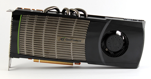
Geforce GTX 480 is a dual-slot card, which is common with high end cards, but it is not quite common seeing a reference card with a heatpipe solution. You’ll notice that in an effort to deliver thermals that would satisfy the GTX 480’s hot ticker, most of the card’s “hood” is actually the heatsink itself and plastic is there mostly for purposes of making sure the heat leaves the case via air outlets on the I/O panel, and that cooler blows towards the heatsink.
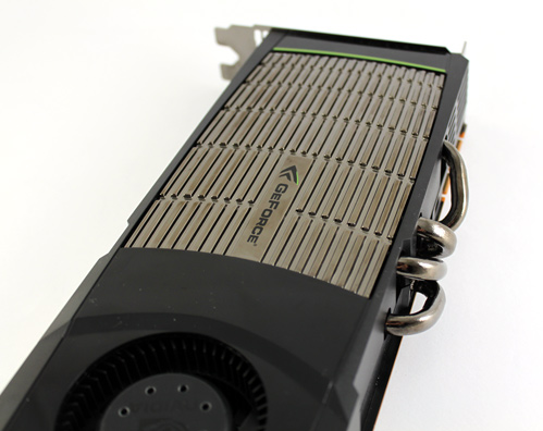
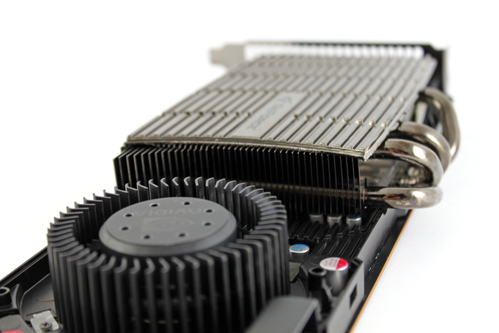
A glance at Geforce GTX 480 would suggest that the card comes with 4 heatpipes, although the card packs 5 in total, as is evident from the picture where we took the plastic hood off. We must admit it looks great with the chrome look and it sure looks like it has what it takes to dissipate heat from the GF100 GPU. GTX 480 has TDP of 250W (at idle consumes about 55W) and it needs external power via one 8-pin and one 6-pin connector. Recommended PSU for the GTX 480 is 600W whereas for GTX 470 Nvidia recommends a 550W PSU (GTX 470 has TDP od 215W).
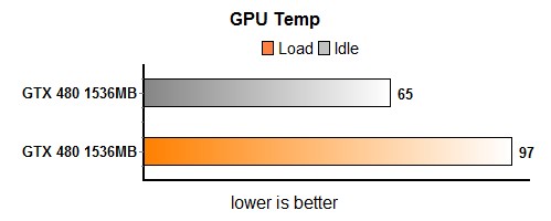
The fan looks much like the one on the current high end Radeon cards, and it can be very loud when GPU is hot. We measured about 65°C in idle mode and about 92°C in 3D with peak at 97°C.
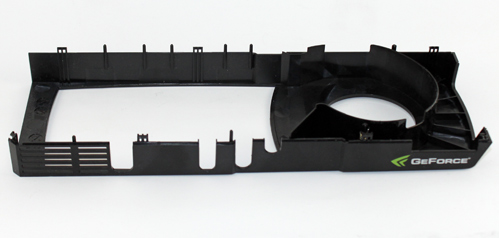
Nvidia was pretty conservative with usage of plastics, as the GTX 480's hood is basically a light frame with big holes in the middle where the heatsink and the fan are placed.
All the power components are cooled by the fan and passive heatsink, as you can see from the following picture. Nvidia is using a Delta fan, which is rated at 1.8 A.
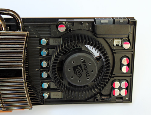
Nvidia resorted to using the same trick they used on the dual-GPU GTX 295 for air supply - this card features a hole in the PCB behind the fan as well. There's also an air outlet on the I/O panel and it's similar to that on the GTX 285.
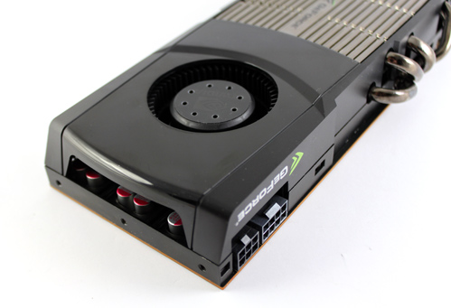
Power connectors are located on the top of the card.
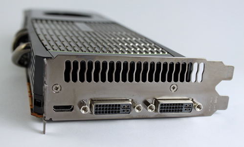
The I/O panel features two standard dual link DVI outs as well as one miniHDMI. Despite the card supporting DisplayPort, Nvidia thought more users will need HDMI, so DisplayPort implementation will be up to partners. GF100 support HDMI 1.4 and everything that's needed in regards to 3D TV etc.
In case you're looking to use three displays with Nvidia 3D Vision technology, you'll have to reach further into your pockets for another card as one card will allow for two displays only.
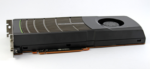
Unlike the GTX 285's cooler, the GTX 480's cooler is pretty easy to disassemble, which will make mounting water cooling easy. If you think that watercooling is overkill in this case, note that three GTX 480 cards get so hot that triple SLI is not advised with air cooling alone.
Today we are finally holding the GTX 480, graphics card based on Fermi architecture. Fermi is the family name for the latest generation of GPUs from Nvidia. The first Fermi derivative is the GF100 GPU - Nvidia’s internal code name for the first Fermi based chip that is used for the GTX 480 and GTX 470 cards. The GF100 is a fairly capable DirectX 11 product manufactured in TSMC's 40nm technology processes with over 3 billion transistors (AMD's RV870, which is used in the ATI Radeon HD 5870, is comprised of roughly 2.15 billion transistors).
Compared to the previous generation GT200, the new GF100 (GTX 480) brings 1.5-3.5x performance gain when compared to the GTX 285 and in addition to greater texture coverage, faster context switching over the GT200, more efficient processing of physics and ray tracing and of course DirectX 11 graphics with unavoidable tessellation which is quite popular these days. According to Nvidia, tessellation is the real reason for the GF100 delay, because Nvidia wanted to have the best implementation.
The biggest advantage of the new GPU is that tessellation and all its
supporting stages are done in parallel, enabling high geometry
throughput. The GF100 tessellation support is 100% hardware, and isn’t
done via software emulation, but even if tessellation is very important
for DirectX 11, actual games based on DirectX 11 that utilize the real
advantage of all its features are still far away and Nvidia has to prove
better performance in current games, and not just in tessellation and
upcoming games.
The GF100 GPUs is composed of a scalable array of Graphics Processing
Clusters (GPCs), Streaming Multiprocessors (SMs), and memory
controllers. The full version of the GF100 chip implements four GPCs,
four Raster Engines, 16 SMs with 32 CUDA cores each and six memory
controllers, but the GTX 480 comes with 15 SMs with total of 480 CUDA
cores and the GTX 470 sports 14 SMs and 448 CUDA cores. Raster Engines
operate in parallel compared to a single Raster Engine in prior
generation Nvidia’s GPUs.
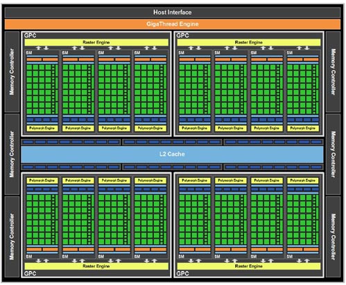
As you can see and conclude from the picture above, one GPC is a dominant high-level hardware block encapsulates all key graphics processing units representing a balanced set of vertex, geometry, raster, texture, and pixel processing resources, what essentially allows each one GPC to function as a full GPU. GPC includes one Raster Engine (for triangle setup, rasterization, and Z-cull) and up to four SMs (for vertex attribute fetch and tessellation).
In its full version, the GF100 has 512 CUDA cores, distributed in 16 SM with 32 CUDA processors for each SM. Every Streaming Multiprocessor has its own dedicated PolyMorph Engine, and four dedicated Texture Units (on GT200 GPU, SMs and Texture Units were grouped together in hardware blocks called Texture Processing Clusters (TPCs)).
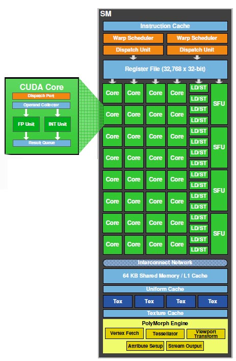
The PolyMorph Engine performs very different tasks and it has five stages: Vertex Fetch, Tessellation, Viewport Transform, Attribute Setup and Stream Output, thus increasing triangle, tessellation and Stream Out performance. Results calculated in each stage are passed to an SM. The SM executes the game’s shader, returning the results to the next stage in the PolyMorph Engine. After all stages are complete, the results are forwarded to the Raster Engines. By having a dedicated tessellator for each SM, and a Raster Engine for each GPC, the GF100 delivers up to 8x the geometry performance of the GT200. Tesselation factor decides on the number of parts that will a certain object be composed of.

The memory interface is 384-bit wide, but GF100 implements six 64-bit GDDR5 memory controllers (384-bit total) to facilitate high bandwidth access to the framebuffer (the GT200 features a wider 512-bit memory interface, but uses GDDR3 memory).
GF100 has 48 ROP units for pixel blending, antialiasing, and atomic memory operations. The ROP units are organized in six groups of eight. Each group is serviced by a 64-bit memory controller.
On-chip L1 and L2 caches enable high bandwidth transfer of primitive attributes between the SM and the tessellation unit as well as between different SMs. Addition of L1 cache helps to keep as much data on the GPU die as possible, without having to access memory. Each SM has 48/16 KB of shared memory (3x that of the GT200), that can be configured as 48 KB of Shared memory with 16 KB of L1 cache, or as 16 KB of Shared memory with 48 KB of L1 cache (there is no L1 cache on GT200).
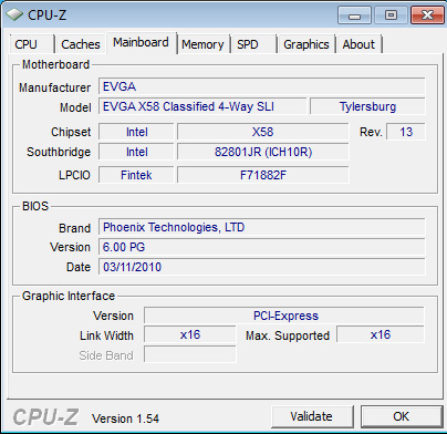
Motherboard: EVGA EVGA X58 Classified 4-Way SLI
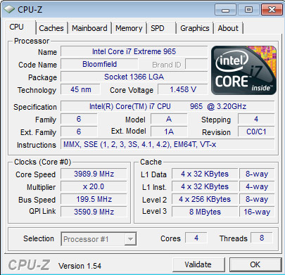
Processor: Intel Core i7 Extreme 965 (provided by Intel);
Memory: 6GB Corsair Dominator 12800 7-7-7-24 (provided by Corsair);
HDD: WD VelociRaptor 300G 10,000RPM (provided by SmoothCreation);
Power Supply: CoolerMaster Ultimete 1100W (provided by Cooler Master);
Case: Obsidian 800D (provided by Corsair);
Fan Controler: Kaze Master Ace 5.25" (provided by Scythe);
Cooler: CoolerMaster V8 (provided by CM)
Operating System: Win7 64-bit;
Driver: Catalyst 10.3 ; Forceware 197.13;
Special thanks to Wolfram from EVGA Europe for supplying us with the motherboard in time to finish this review.
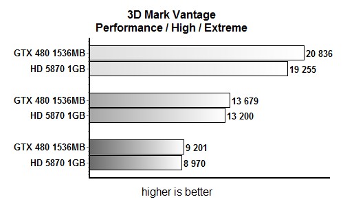
In Vantage benchmarks, Fermi wins hands down. The advantage melts from 8.2% in Performance to 3.6% in High and ends up at 2.5% in Vantage Extreme, but it still manages to beat the HD 5870 in every single test, albeit with a rather tight margin.
DirectX 11 brings some new features with the most important trio consisting of tessellation, multithreading and DirectCompute, which will provide an overall more immersive gaming experience. DirectCompute is perhaps the most important feature of DirectX 11, as it is important for almost any type of application that has to deal with large amounts of data and for gamers too. When it comes to tessellation probably new DirectX 11 games will benefit mostly from it.
Tessellation allows increasing polygon complexity by dynamically subdividing the wireframe of 3D objects when objects are rendered to appear in close-up view while objects that are rendered in the distance need less detail. With tessellation, we can enjoy richer and sharper graphics with quality LOD (Level of Detail) in game while ensuring best possible performance behind the scenes.
Tessellation functionality is implemented and supported by DirectX 11 compatible graphics cards, which in combination with High Definition Displacement Maps can significantly increase the level of detail on most 3D objects. Nvidia's Fermi architecture and its first hardware offspring, the Geforce GTX 480 and GTX 470, supports Microsoft’s latest API and of course hardware tessellation, which Nvidia has targeted as one of the main ways it can differentiate the GF100 from the competition. It seems that Nvidia worked hard to ensure that we get the best implementations for tessellation, and we’ll know soon enough.
In the recently launched 2.0 version, Unigine benchmark shows how tessellation could be implemented in future games. Tessellation factor can altered real time, which directly affects image quality. There’s also extreme tessellation mode that shows mass tessellation, which probably won’t be implemented in games anytime soon. The following tables show why Nvidia is so excited by tessellation – the GTX 480 is simply better at it than the HD 5870.
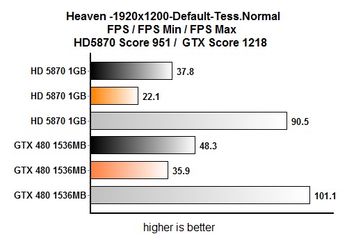
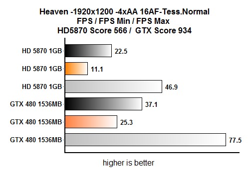
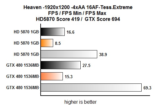
Note beforehand that Unigine 2.0 uses tessellation levels that won't be implemented in games anytime soon, and so this benchmark is more for comparison purposes rather than just seeing which card churns out more frames.
Unigine 2.0 at 1900x1200 and normal tessellation sees the GTX 480 outpacing the HD 5870 by about 28%. It's well worth noting that minimum recorded fps on GTX 480 is 62% better than the HD 5870.
As soon as 4x antialiasing and 16x anisotropic filtering are turned on, the GTX 480 ends up with a 64.21% average advantage and it even hits a 127% better minimum fps.
The last Unigine 2.0 test runs at 1900x1200, 4xAA and 16xAF, which is identical to the previous test except for using Extreme tessellation. Strangely enough, while the GTX 480 again ends up about 64% faster, it seems that it takes a harder fps hit than the HD 5870. Compared to same scenario with normal tessellation, the GTX 480 takes a hit of about 10 fps whereas the HD 5870 drops by about 6 fps.
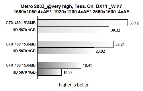
Strapped with 1536GB of fast GDDR5 memory, Nvidia GTX 480 has no trouble dealing with high resolutions and tessellation in undoubtedly one of the best looking PC games of 2010, Metro 2033. Metro 2033 is post-apocalyptic game developed by 4A Game and implements a number of advanced DX11 features with the latest generation of DX11 graphics cards.
Far Cry 2
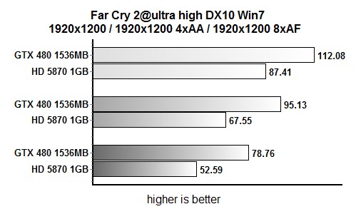
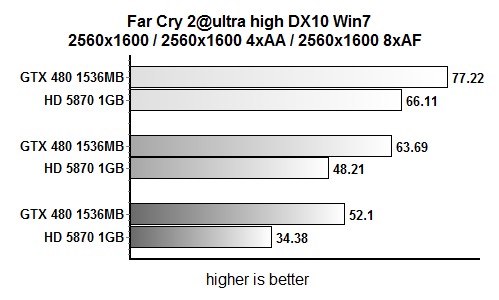
As you can see, in Far Cry 2 at ultra high settings, the GTX 480 is definitely faster than the HD 5870 and there is no question about it. When the AF and AA comes into play, the GTX 480 definitely shows its sheer power and the difference is quite obvious at a higher resolutions.
Crysis
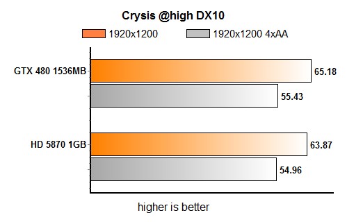
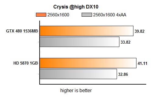
Crysis was a game that certainly knew how to put some pressure on the GPU, and you can see that even Fermi is having a tough time with the game itself. In this case, GTX 480 is on a par with the HD 5870 and even looses when the resolution is pushed higher.
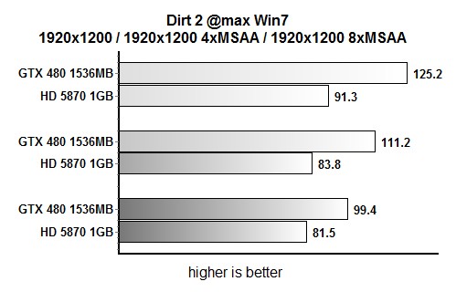
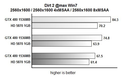
Dirt2
Yet again, GTX 480 shows its sheer power and it is faster than any single GPU. The difference between cards isn't that big, but after all Dirt 2 is the game where ATI's HD 5870 really shines, especially with Catalyst 10.3 drivers.
Batman: Arkham Asylum
Batman: Arkham Asylum is one game that Nvidia really likes to brag about and it certainly looks impressive with PhysX as it could be the only game that really adds that final touch to the overall feeling and gameplay.
Without PhysX
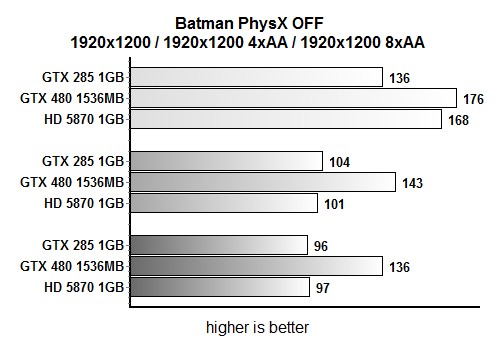
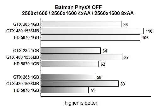
Even without PhysX the GTX 480 is the king of the hill, especially if you add some quality with AA and AF. This didn't came as a surprise considering that GTX 285 is doing a hell of a job in this game with or without PhysX and the GTX 480 was designed to be much faster than the GTX 285.
With PhysX
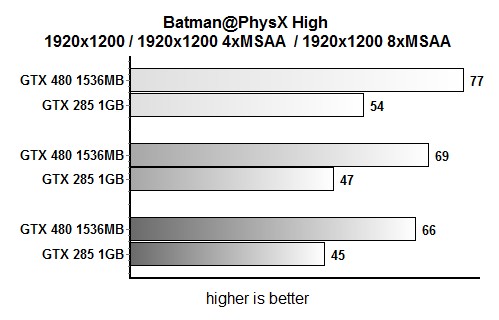
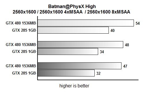
When PhysX is enabled you can clearly see how much faster is the GTX 480 when compared to the GTX 285. Even at higher resolutions we are quite sure that GTX 480 could possibly give a playable framerate.
Well, was Fermi worth the wait?
The most anticipated graphics card is rather interesting, and no one can argue the fact that it is the fastest single-GPU card on the market. On the other hand, it is also the most complex piece of graphics silicon that was ever created, and at 3.2 billion transistors it is certainly the most impressive one.
The GF100 is designed for future games based on DirectX 11 specs, and it bets on the importance of DirectX 11 tessellation coupled with a significant geometric performance increase but today it cannot shine. It is faster than any single-GPU card graphics card and performs quite well in new DirectX 11 tests. Compared to the GT200 generation, the new GPU offers several major improvements. Physics processing is now more efficient, as well as ray tracing. Let's not forget tessellation, either.
However, while the state of the art architecture is something to drool over, real life tests and economics work against the GTX 480. In most scenarios it is 20 to 25 percent faster than the HD 5870. On the other hand, AMD's HD 5870 is available for about €330, while the GTX 480 will set you back €450. So, the architecture gets our thumbs up, but the actual card leaves much to be desired. While it is somewhat faster than the HD 5870, it's pricey, hot and it needs quite a bit more power than the HD 5870. The fact that an HD 5970 costs €515 also works against it.
It is possible the GTX 480 will manage to outpace AMD's 5000 series cards by a wider margin in new games, and a 512-shader version could help turn the tables. Although Nvidia is back in the game, it still has a long way to go.
